Memory Hierarchy Overview with Capacity, Performance, and Power Implications
14 Oct 2023An application (software) is a sequence of instructions executing data operations. The instructions and data are stored in some form of memory. The computation logic within a processor (core) can only be surrounded by a few KBs of memory (registers) due to physical area and wiring constraints. As a result, to store more data and programs, we need a larger memory.
In an ideal world, we have infinite memory, available instantly (1 processor cycle) to the computation logic in the processor. A single access to data in a large memory (~TB capacity) like a hard disk with mechanical moving parts can take milliseconds. A millisecond is $2 \times 10^6$ cycles for a processor running at 2 GHz clock frequency!
Clearly, any performance optimization we do for a processor core in terms of its process/design/architecture is only helpful once we optimize for the memory latency.
On the other hand, what happens to power consumption when the processor is waiting for the data from memory? The processor core is stalled, and without any power management, it wastes power during that time. Therefore, memory access latency optimization is not only critical for improving performance but also for improving energy consumption.
At the heart of memory hierarchy, there are two assumptions for memory access of modern programs:
-
Temporal Locality - We are more likely to re-use the same data shortly after using it once.
-
Spatial Locality - We will likely use the surrounding data points (bytes) to access current data.
These assumptions lead to a cache-based design, i.e., adding multiple memories between the fast registers closest to the processor core and the hard disk.
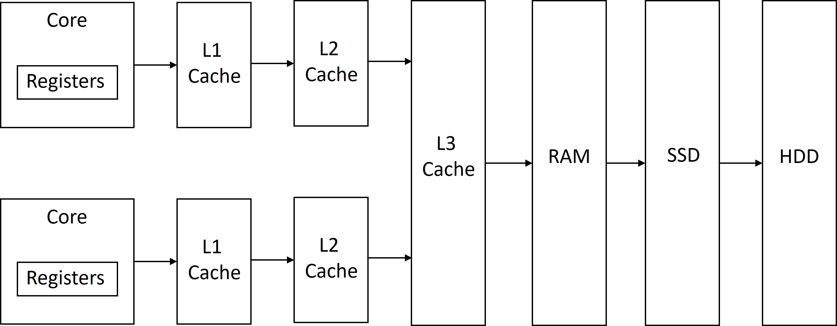
The figure below shows an example of a modern memory hierarchy. First, we have the computational logic in the core that is closest to registers, then we have L1 cache ($), L2 cache, L3 cache, Random Access Memory (RAM), Solid State Drive (SSD), and Hard disk drive (HDD).
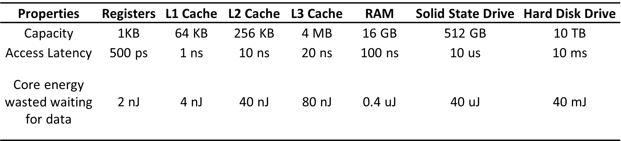
The table below shows an example of capacity, access latency, and the core energy wasted while waiting for data from memory. I used Hennessy and Patterson’s computer architecture book for some of these capacity and latency numbers.
Computation of Core Energy
For simplification, assume the core is running at 2 GHz clock frequency, its Dynamic capacitance is 1 nF, voltage is 1 V, and leakage power is 50% of the total power consumption.
Dynamic Power: $P_{Dynamic} = C_{dyn} V^2 f = 1nF \times (1V)^2 \times 2\times 10^9 Hz = 2 W $
Total Power: $P_{total} = P_{Dynamic} + P_{leakage} = P_{Dynamic} + 0.5 \times P_{total}$
We can solve this equation to get, $ P_{total} = P_{Dynamic}/0.5 = 2/0.5 W = 4 W $
Without any power management like Dynamic Voltage Frequency Scaling or Sleep states, when the core waits for data for T time, the energy wasted = $P_{total} \times T$.
Latency Improvement of the Hierarchical Memory Architecture
The program can still go to a Hard disk (HDD). So, how did the latency improve by adding more memories?
Well, that is where the temporal and spatial assumptions on the data kick in. For modern applications, most data access would happen closer to the computational logic in the core. If the data is absent in the closest memory, it would go to the next memory in the hierarchy. This really becomes a game of probability.
Consider a program with a 90% hit rate in the L1 cache, 5% in the L2 cache, 4% in the L3 cache, 1% in the RAM. The total latency can be computed as follows:
\[Latency_{hierarchy} = 90\% \times L1_{access-latency} + 5\% \times L2_{access-latency} + 4\% \times L3_{access-latency} + 1\% \times RAM_{access-latency}\] \[Latency_{hierarchy} = 0.9ns + 0.5ns + 0.8ns + 1ns = 1.22 ns\]Consider the case when we only had registers and the RAM (no cache). Then, 100% of hits would be in the RAM for the same application. The latency in this case will be 100 ns, which is much larger than 1.22 ns!!