17 Oct 2023
Compulsory miss, Capacity miss, and Conflict miss for a Cache are already well documented in the literature.
The main question is how do we measure what is causing the cache misses in our system? Can we do something about it? Do we need to increase the cache size? Or change the cache eviction policy?
If it is a compulsory miss, there is nothing we can do. We can measure such misses by simulating a case with an infinite cache.
Next, we can determine if our cache size is sufficient using a fully set-associate Cache. Here, we replace the least recently used Cache block. Any additional misses over the compulsory misses are due to the cache size. We can optimize for these misses by increasing Cache size.
Finally, the remaining misses in the system would happen due to other assumptions on the Cache architecture, such as n-set-associativity and Cache eviction policies. We can change these to optimize for a given set of workloads.
17 Oct 2023
The CPU core will generally send an instruction to load data from some main memory (RAM) address. How would this main memory address be modified for cache access?
The memory address is divided into three parts - Set Index, Block Offset, and Tag.
Consider a cache as a table storing data. A set is a row in a Cache memory table. The block or cache line size is generally 64 bytes. One set (row) of the Cache stores a cache line or a block. One column of the cache memory table stores 1 byte of data. This implies we have 64 columns. How do we know the number of sets?
The size of cache memory table = Number of sets $\times$ Block size
Assume a 64 KB Cache size. The number of sets (or rows in the table) for this Cache is 64KB/64B= 1024.
Next, let us answer how many bits in our main memory address are used for our Cache with 1024 set of blocks size 64 bytes. Consider a main memory address of 32 bits. To identify a unique row in the table (set), we need 10 bits index, since the number of sets = 1024. Similarly, we need 8 bits offset to uniquely identify each of the 64 columns of a block.
Out of the 32 bit, we only need the lower 10+8 = 18 bits to address the Cache. What about the rest of the 32-18 = 14 bits?
As you can notice, two unique 32-bit addresses with the same lower 18 bits can map to the same cache cell. This is expected because a cache size is a subset of the main memory size. We store the rest of the 14 bits as a tag. When we access one memory address, we reserve its full Block in the set and keep its tag in the tag directory (number of rows = number of sets). Next time, we will have a Cache hit when we access another memory address within the same Block. If we access a new memory address with the same set and block offset but a different tag, we call it a cache miss. Then, go to main memory, fetch that entire Block with new tag, and store it in the same set index.
So far, the type of Cache we looked at is called a direct mapped cache (a.k.a. 1-way set associative Cache). Notice the extra power we burn in storing the tags.
Set Associative Cache
We can store multiple tags in a single row of the cache table. A 2-way set associative cache would mean we store two tags and two blocks of Cache for each row in the table. In this case, the number of sets will drop to half for the same cache size. The address decoder logic will become more complicated, and we will store two times more tags. As a result, we will burn more power.
However, this can increase performance (higher hit rate) because we do not have to evict the older Block with a different tag. In our temporal locality case, if we access that same Block sometime very soon, it is nice to have it stored in the Cache instead of evicting it for another Cache block.
Similarly, a n-way set associative Cache can be built. Each set will have n-Cache blocks. The power consumed is way higher in this case, so performance gains might not be significant.
In an extreme case, we can even construct a fully associative cache! Use a single set with all Cache blocks and directly compare tags to see which one needs access. The main memory address will not require a Set index field for this case. The number of Cache blocks will be determined by the Cache size. Correspondingly, we will choose the number of Block offset bits in the address.
14 Oct 2023
An application (software) is a sequence of instructions executing data operations. The instructions and data are
stored in some form of memory. The computation logic within a processor (core) can only be surrounded by a few KBs of memory (registers) due
to physical area and wiring constraints. As a result, to store more data and programs, we need a larger memory.
In an ideal world, we have infinite memory, available instantly (1 processor cycle) to the computation logic in the processor.
A single access to data in a large memory (~TB capacity) like a hard disk with mechanical moving parts can take milliseconds.
A millisecond is $2 \times 10^6$ cycles for a processor running at 2 GHz clock frequency!
Clearly, any performance optimization we do for a processor core in terms of its process/design/architecture is only helpful once we optimize for the memory latency.
On the other hand, what happens to power consumption when the processor is waiting for the data from memory? The processor core is stalled, and without any power management, it wastes power during that time. Therefore, memory access latency optimization is not only critical for improving performance but also for improving energy consumption.
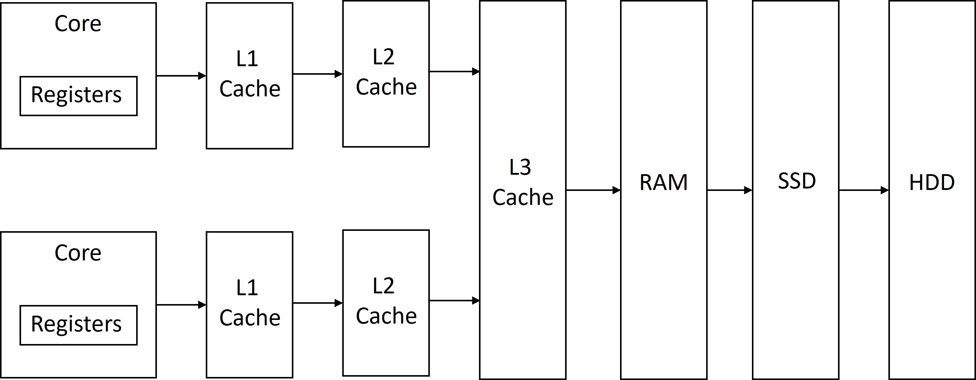
At the heart of memory hierarchy, there are two assumptions for memory access of modern programs:
These assumptions lead to a cache-based design, i.e., adding multiple memories between the fast registers closest to the processor core and the hard disk.
The figure below shows an example of a modern memory hierarchy. First, we have the computational logic in the core that is closest to registers, then we have L1 cache ($), L2 cache, L3 cache,
Random Access Memory (RAM), Solid State Drive (SSD), and Hard disk drive (HDD).
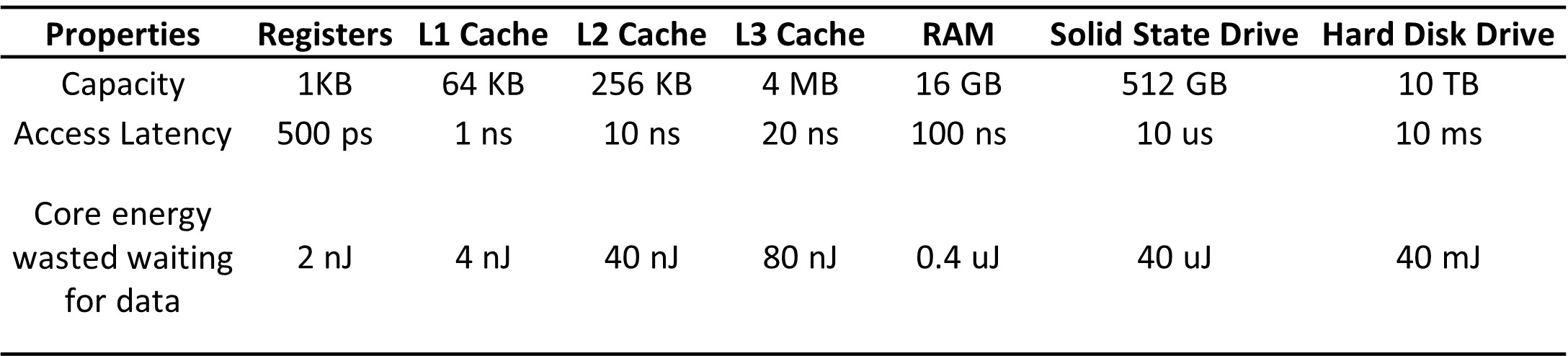
The table below shows an example of capacity, access latency, and the core energy wasted while waiting for data from memory. I used Hennessy and Patterson’s computer architecture book for some of these capacity and latency numbers.
Computation of Core Energy
For simplification, assume the core is running at 2 GHz clock frequency, its Dynamic capacitance is 1 nF, voltage is 1 V, and leakage power is
50% of the total power consumption.
Dynamic Power: $P_{Dynamic} = C_{dyn} V^2 f = 1nF \times (1V)^2 \times 2\times 10^9 Hz = 2 W $
Total Power: $P_{total} = P_{Dynamic} + P_{leakage} = P_{Dynamic} + 0.5 \times P_{total}$
We can solve this equation to get, $ P_{total} = P_{Dynamic}/0.5 = 2/0.5 W = 4 W $
Without any power management like Dynamic Voltage Frequency Scaling or Sleep states, when the core waits for data for T time,
the energy wasted = $P_{total} \times T$.
Latency Improvement of the Hierarchical Memory Architecture
The program can still go to a Hard disk (HDD). So, how did the latency improve by adding more memories?
Well, that is where the temporal and spatial assumptions on the data kick in. For modern applications, most data access would happen closer to the computational logic in the core. If the data is absent in the closest memory, it would go to the next memory in the hierarchy. This really becomes a game of probability.
Consider a program with a 90% hit rate in the L1 cache, 5% in the L2 cache, 4% in the L3 cache, 1% in the RAM. The total latency can be computed as follows:
\[Latency_{hierarchy} = 90\% \times L1_{access-latency} + 5\% \times L2_{access-latency} + 4\% \times L3_{access-latency} + 1\% \times RAM_{access-latency}\]
\[Latency_{hierarchy} = 0.9ns + 0.5ns + 0.8ns + 1ns = 1.22 ns\]
Consider the case when we only had registers and the RAM (no cache). Then, 100% of hits would be in the RAM for the same application. The latency in this case will be 100 ns, which is much larger than 1.22 ns!!
03 Oct 2023
I always loved teaching, whether hands-on microcontroller tutorials as an undergraduate student or as a Teaching Assistant in graduate school. In fact, that is why I pursued a Ph.D. so that I can teach in Academia. Eventually, I became interested outside of Academia and gravitated toward an industry job with more immediate impact.
Still, the teaching bug inside of me never died. I kept finding a setup to easily record and upload lectures online. Recently, I found one of the easiest methods to do this, requiring much less setup time.
-
Hardware: iPad (any basic model will do) + Apple pencil
-
App: Notability
-
Video Editing: ScreenPal (may not be the best)
-
Video publishing: Youtube
Here is the link to my first video
11 Dec 2022
When we think about choosing a computer’s memory (RAM), we often think about the type, such as DDR4 or DDR5, size (measured in GBs), and speed (measured in MT/s).
When you are building a PC yourself, it is important to know some additional memory parameters to carefully optimize your system and get the best performance, such as the memory timing, power and voltage.
Among these, the the memory timings are critical because they determine the performance and speed of the memory.
The memory controller in the CPU plays a critical role in managing the memory, but it relies on the memory timings to know how long to wait for the data to be available, how long to keep the row selected, and how long to wait between refresh cycles. If the memory timings are incorrect or not optimized, the memory may not be able to operate at its maximum speed, which can result in slower performance and reduced efficiency. Therefore, it is important to carefully set and optimize the memory timings in order to ensure that the memory can operate at its maximum speed. Memory timings are typically measured in nanoseconds (ns) or clock cycles. The specific memory timings used can significantly impact the system’s overall performance, so manufacturers carefully optimize them to ensure that the memory can operate at its maximum speed. Memory timings are typically specified as a series of numbers, such as “40-40-40-77” or “9-9-9-24,” representing the different delays and intervals in accessing the memory.
As an example, the “9-9-9-24” memory timing refers to a specific set of memory timings that are used to determine the performance and speed of a computer’s memory (RAM). The four numbers in this timing specification represent the values of four different memory timing parameters, as follows:
-
The first number (9) represents the CAS (Column Address Strobe) latency, which is the delay between the time a memory request is made and the time the data is available for reading or writing.
-
The second number (9) represents the RAS (Row Address Strobe) to CAS delay, which is the delay between the time a row of memory is selected and the time the data in that row is available for reading or writing.
-
The third number (9) represents the RAS pulse width, which is the minimum amount of time that a row must be selected in order to access the data in that row.
-
The fourth number (24) represents the RAS to precharge delay, which is the delay between the time a row is no longer being accessed and the time it is precharged (i.e. the charge is removed from the row).
Here is a fantastic reference for that explains these parameters in some more detail.
When building a PC, I got a DDR5 (2x16 GB to utilize both channels of memory controller) 4800 MT/s memory at 1.1 V. The maximum memory speed supported by my CPU is 4800 MT/s, so I was confident that this was what I needed. However, after I finished the build, the memory speed was only 4000 MT/s. That led me to investigate this further. The BIOS will put the memory in a safer operating zone of 4000 MT/s, and we have to change the memory timings to get maximum performance. Typically, RAMs support Extreme Memory Profiles (XMP) profile that auto lists the memory parameters optimized to get maximum performance. It is as easy as selecting a simple option in BIOS and being done with it. However, in my case, the memory was not XMP read (even though the packet said it was). As a result, I had to rely on the JDEC specification, which had the timing parameters for 4800 MT/s. However, when I tried those parameters, the BIOS hung, and I had to reset it. Then, I got another memory same company and product, except it was rated as 5200 MT/s speed and 1.25 V. This new RAM worked at maximum performance since it had the XMP, and I could enable it.